

I’ve worked with the PN532 before.
The first version of NullTag actually worked. It could read cards, clone some tags, dump memory — the usual stuff. But deep down I knew it wasn’t engineered properly. It was an ESP32, a PN532 module, some wiring, a display… it did the job, but it didn’t feel like a real device.
So I never open-sourced it.
It felt like a prototype pretending to be a product.
This time, I decided to rebuild it properly. No breakout modules. No ready-made antenna boards. Just custom PCBs and real RF design.
And that’s where things got interesting.
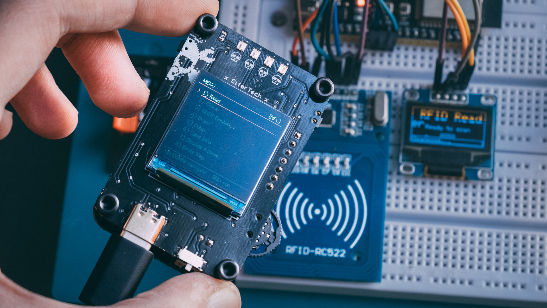
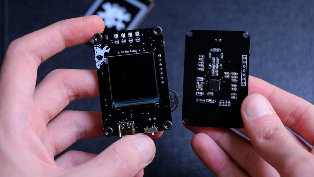
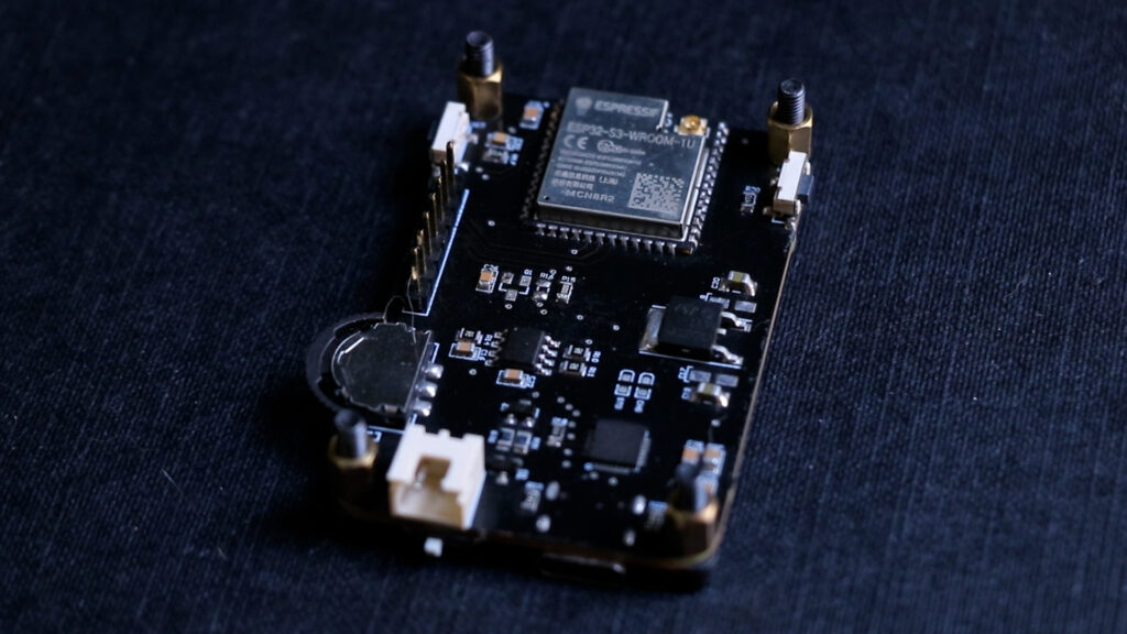
🧠 The New Hardware — Three Boards, One Purpose
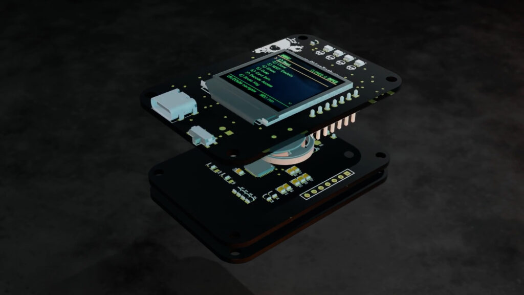
NullTag v2 is built as a three-piece PCB stack.
The main board handles logic and UI. It includes:
✅ ESP32 MCU
✅ 240×240 TFT LCD (ST7789 driver)
✅ Dedicated power management circuitry
✅ 3-way hardware switch
This board is stable. It works. No drama there.
The second board is dedicated to the PN532. No module this time — just the chip and the required supporting components, connected over SPI.
The third board is the antenna. Just the antenna. A custom PCB coil designed for 13.56 MHz.
Separating the antenna was intentional. RF design is unpredictable. If I need to tweak the coil geometry or matching components, I don’t want to respin the entire main board.
That decision turned out to be very important.
🧩 Firmware
This isn’t an Arduino demo sketch anymore.
The firmware is structured:
-
• 📟 TFT menu-driven interface
-
• 🔘 3-button navigation (UP / DOWN / SELECT)
-
• 🔌 PN532 over SPI
-
• 🖥 Terminal-style diagnostic output
-
• 📡 Reader + Target mode support
-
• 🔍 Clear bring-up validation
On boot, the system checks communication with the PN532. If SPI fails, it stops and shows an error. No guessing.
Menus are navigated with three buttons. The display has a terminal-style interface. It feels like a device, not a dev board with a screen attached.
Feature-wise, it includes:
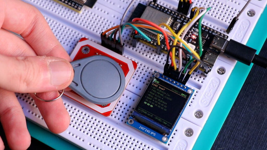
📖 1) Read
Reads ISO14443A tags, captures UID, identifies likely card family (Classic, Ultralight, NTAG, DESFire heuristic), and reads accessible blocks/pages.
🧬 2) Clone
Performs full source tag read and target write flow.
Includes authentication attempts and write verification.
Success depends on tag compatibility and key access.
🧹 3) Erase
Authenticates writable regions and clears memory where allowed.
Respects lock bits and card permissions.
📦 4) Dump
Reads sequential sectors or pages and exports structured hex data over serial.
Reports read failures when access conditions block memory.
📋 5) Card Info
Displays:
-
• UID length
-
• UID value
-
• Detected card family
Uses anti-collision and behavioral probing to classify tags.
🔐 6) Decode Access
Parses MIFARE access-condition bytes and translates bitfields into readable permissions.
No more raw hex confusion.
⚠️ 7) Disrupt Tag
Executes aggressive authentication and write patterns for resilience testing.
Can permanently alter tags.
Intended only for disposable test media you own.
⚠️ 8) Disrupt Emulator
Uses PN532 target mode to generate edge-case or non-standard responses.
Designed for testing reader robustness and error handling.
📊 9) Scan UIDs
Continuously polls for nearby tags.
-
• Converts UID bytes to hex
-
• Stores unique set in memory
-
• Updates live counters
-
• Logs over serial
Perfect for antenna validation.
🔎 10) MIFARE Audit Mode
Attempts default/common key validation and access-path testing.
Designed strictly for authorized security evaluation.
🔁 11) Reader Emulation Test
Validates PN532 initiator/target transitions.
Tests APDU exchange behavior and timing compatibility.
📋 12) Card Audit
Combines:
-
• Type detection
-
• Memory sampling
-
• Default-key probing
-
• Configuration consistency checks
Into a compact security summary.
Some of these are for lab use only. Some are for auditing. But the goal is simple: turn NullTag into an NFC research platform, not just a reader.
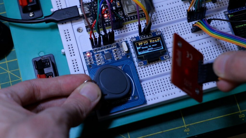
⚡ The Moment Everything Looked Perfect
Power it on. Display initializes. ESP32 boots cleanly. SPI communication works. PN532 firmware version detected successfully.
That moment feels good. Everything digital is alive.
You scroll through the menu, select “Scan UID,” bring a tag close…
Nothing.
No UID.
No response.
No activity.
That’s when you realize this isn’t a firmware problem.
It’s RF.
📡 The Antenna Reality
NFC runs at 13.56 MHz. At that frequency, tiny mistakes matter.
The antenna and matching network form a resonant circuit. If it’s even slightly off, the field strength drops dramatically. You might still see perfect SPI communication. The chip might respond to commands. But the RF field won’t be strong or stable enough to power and communicate with a tag.
And when that happens, it fails silently.
I went through the documentation again. Checked the reference design. Recalculated matching capacitors. Reviewed the layout. Adjusted components.
Still no progress.
That’s when you understand something important:
Digital systems fail loudly.
RF systems fail quietly.
And quiet failures are harder.
🌐 Matching Network — The Part Nobody Talks About
Between the PN532 and the antenna sits the matching network.
Its job is to transfer power efficiently and tune the system to resonate at exactly 13.56 MHz.
Too high Q factor? The system becomes unstable and narrow-band.
Too low Q? The field is weak.
Wrong capacitor values? No resonance.
Bad layout? Losses everywhere.
You can copy values from a reference schematic, but if your coil geometry is different, those values are just guesses.
That’s the stage I’m in right now — iteration.
Measure. Adjust. Test. Repeat.
This is normal in RF work. It just doesn’t look glamorous on camera.
🔍 Debugging — Eliminating the Wrong Suspects
First thought: maybe SPI is unstable.
Checked it with logic analysis. Clean.
Second thought: maybe PN532 initialization is incomplete.
Firmware version reads correctly. Chip responds properly.
Third thought: antenna and matching network.
And that’s where the focus shifted.
Once you eliminate digital failure, you’re left with physics.
🔩 Why I’m Doing It This Way
I could have just used a PN532 breakout again.
It would have worked immediately.
But that wouldn’t teach anything.
Designing your own antenna and tuning it forces you to understand what’s actually happening at the RF level. It’s uncomfortable. It requires patience. It sometimes makes you question your layout skills.
But it’s real engineering.
NullTag v2 isn’t just about making a tool. It’s about building something from the ground up and understanding every layer of it — from SPI communication all the way to electromagnetic resonance.
 Sponsored by NextPCB
Big thanks to NextPCB for supporting this project!
If you’re building your own ESP32-DIV or any other PCB project, I highly recommend NextPCB for fast, reliable, and affordable PCB manufacturing and assembly.
 Get your boards made here → https://www.nextpcb.com
🧩 Where It Goes From Here
The plan is simple:
-
• Tune the antenna properly
-
• Adjust matching network values
-
• Possibly redesign coil geometry
-
• Validate range and stability
-
• Then refine firmware
The main board works. The firmware works. The PN532 communicates.
Now it’s just a matter of getting the RF section right.
And once it locks in, NullTag v2 becomes what it was supposed to be from the start: a clean, custom-built NFC research handheld.